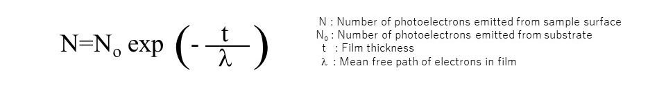
This example shows the measurement of silicon wafers on which thermal oxide films of differing surface thicknesses are formed.
Fig.1 Measurement example of silicon wafers with different
thickness of oxide film formed on the surface
The oxide film is a thermal oxide film formed by the rapid oxidization method. Film thickness was measured using an ellipsometer. We see that the slope of the graph becomes smaller as the thickness of the oxide film increases. This is because electrons emitted from the substrate silicon are attenuated as they pass through the thermal oxide film.

Fig.2 Difference between photoelectron emission
with and without surface coating
The following equation gives the count rate N for electrons counted after passing through the thermal oxide film.
As shown in Fig. 3, the relationship between thermal oxide film thickness and the logarithm of the photoelectron count rate is linear.

M.Uda "Open counter for low energy electron
detection", Jpn. J.Appl. Phys. 24 (1985) 284.
Fig.3 Relationship between the thickness of silicon oxide
film and the count rate of photoelectrons
The thickness of extremely thin oxide films less than 100 Å (10 nm) thick formed on the silicon surface is measured using vacuum systems such as XPS. However, this process is laborious and time-consuming. For this reason, it is not suitable for examinations in production settings. If a number of samples are prepared with differing thermal oxide film thicknesses and measured using XPS, then measured as datum samples with the AC-3, we can create calibration curves like those shown in Fig. 3, allowing subsequent use of the AC Series for rapid testing of oxide film thickness.