Operation and ionization potential of organic light-emitting diode devices
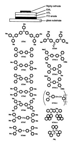
The figure below shows a cross section of an organic light-emitting diode (OLED device).
The device consists of an organic layer that emits light when a current flows through it, sandwiched between a metal cathode and an ITO transparent anode made of a transparent conducting material such as indium tin oxide (ITO).
These are then formed as laminated layers of nanometer-scale thickness on a glass substrate.
Applying a positive voltage to the anode and a negative voltage to the cathode causes electrons to flow from the metal cathode into the organic layer.
Meanwhile, holes from the ITO anode flow into the organic layer.
The electrons and holes reunite, generating light (photons).
Let’s examine the flow of holes from the ITO anode into the organic layer.
The figure on the right is an energy diagram for the boundary between the ITO and organic layer.
Holes close to the ITO Fermi level flow into the HOMO level of the organic layer.
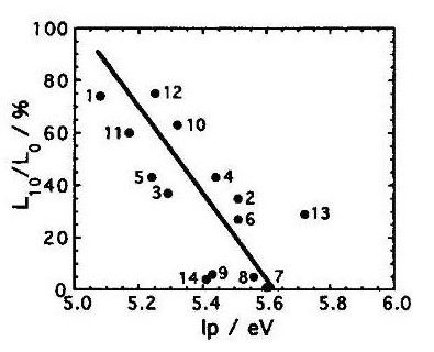
The energy difference between the ITO Fermi level and the organic layer HOMO level forms a barrier to hole flow.
This corresponds to the difference between the work function (WF) of the ITO and the ionization potential of the organic material.
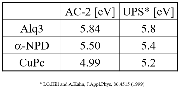
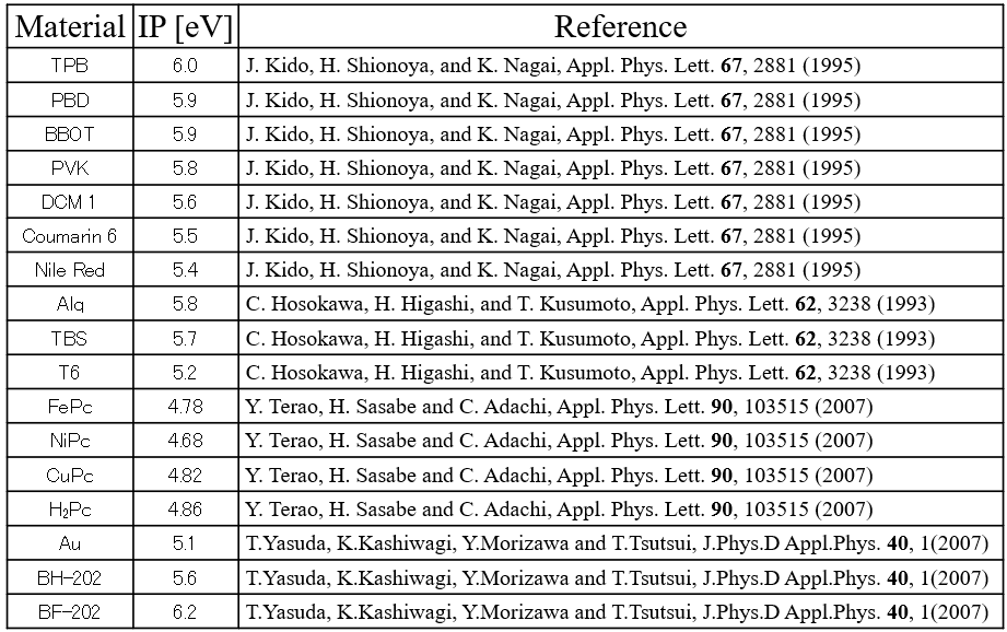
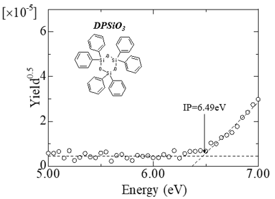
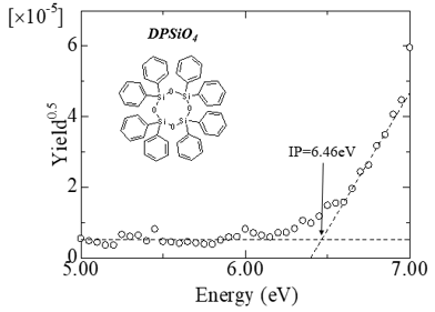
When designing OLED devices, the capacity to estimate the work function and ionization potential of the material is of critical importance.
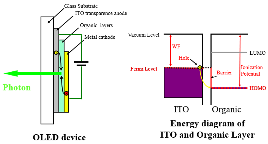
Fig.1

